PKG
- FCBGA
- FCCSP
- CSP
- SIP, AIP
- FCBOC
FCBGA (Flip Chip Ball Grid Array)
Applications
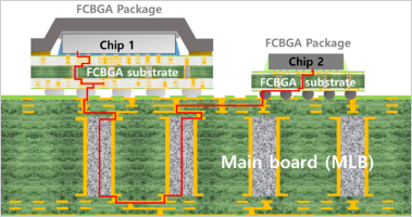
It is mainly used for CPU and ASIC semiconductor packaging. BGA substrates connect the chip and the board using solder bump, which allows more wiring and a faster speed than gold wires.
Key features
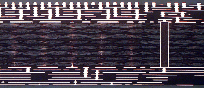
Flip chip ball grid array (FCBGA) requires applying a multilayer build-up technique for 16 layers or more, forming super-fine circuits less than 10 um, forming solder bumps below 130 um, and manufacturing large-area substrates bigger than 60 x 60 mm.
Daeduck’s exclusive FCBGA production line is working on the development and mass production with the aim of reaching the technological standards necessary for FCBGA such as automotive MPU, high-speed communication chip, and data center processor.- FCBGA packages electrically connect with solder bumps on the chip, and protect the chip from external factors.
- Daeduck’s FCBGA substrates are cutting-edge multilayer PKG Substrate applied with the build-up technique and SAP technology, and it provides a basic foundation and electrical connection paths for FCBGA packages.
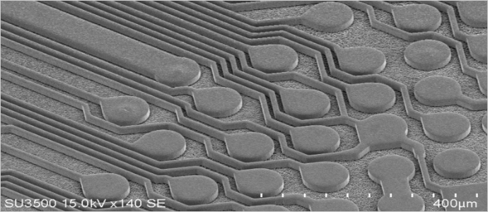
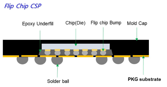
FCCSP (Flip Chip Chip Scale Package)
Applications
Flip chip chip scale package (FCCSP) is widely used in, and is designed for, high-speed/RF packaging where electrical performance is essential, such as mobile AP, high-performance work station, server, data communication product, Internet router, and so on.
Since there is no wire bond roof, the distance and connection to die is small, which enables the maintenance of inductance with a high density, and determination of electric paths that are optimal for high-frequency signal lines. For this reason, it can be applied in a wide range of fields.Key features
Unlike the conventional wire bonding method, FCCSP does not use wires, and directly connects bumps between chip-package substrates, allowing improved electrical performance, increased density, and miniaturization through the elimination of wire space.
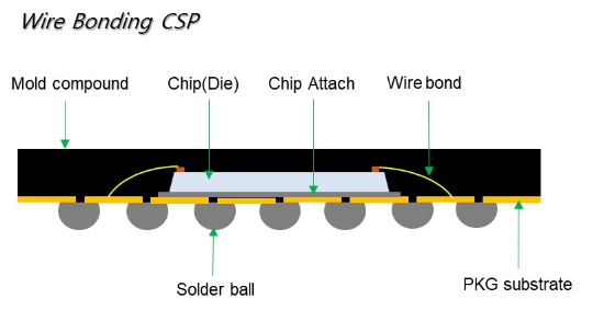
CSP (Chip Scale Package)
Applications
Chip scale package (CSP) refers to a product where the surface of the chip accounts for more than 80% of the package area. Main applications include flash memory and mobile DRAM products.
Key features
Thin structure
As slimming of substrates increases the risk of defects in the product drive, materials with high stiffness are used to ensure the product driveability, and to increase the ease of mass production.Warpage control
The thermal conditions and volume of substrates are controlled to manage warpage of substrates.
- MASS
- SAMPLE
Structure 2L ~ 6L 2L ~ 6L Substrate
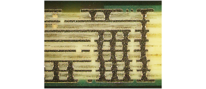
Thickness2L 80㎛ 75㎛ 3L 80㎛ 70㎛ 4L 110㎛ 100㎛ Bond finger Pitch 60P (32/15, Ni 3) 55P (25/15, Ni 2) Line Width/Space (/w mSAP) 40Pitch (20/20㎛) 32Pitch (16/16㎛) SR Registration 15㎛ 12㎛ SiP (System In Package)
Applications
System in package (SiP) refers to a module that contains a functional unit. Commonly comprised of one or more wire-connect or Flip-chip Semiconductors, passive elements, etc, and by consolidating diverse functions into one Package, reduce system size, and improve function and reliability.
Applied to RF, Wireless installation(Power Amp. GPS Module, Cell), Networking and Computing etc.Key features
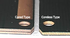
Coreless substrates, which do not use a core layer, can be made even slimmer.
A coreless substrate can be made slimmer than a cored substrate by making the substrate only using build-up layers.
In addition, this method also increases the overall inductance and signal reliance of the package.
Cored Type

Coreless Type
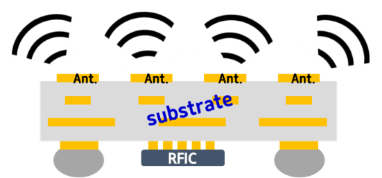
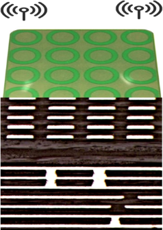
AiP (Antenna In Package)
Applications
Antenna in package (AiP) is a substrate with built-in antenna function. It is a substrate solution that integrates various electronic parts and communication modules including transmission/reception chipset, filter, and power amplifier into a single antenna package.
Key features
It is a package product in an AiP form factor. The substrate contains the antenna for 5G transmission and reception in line with the spread of 5G smartphones.
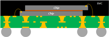
Since the antenna is built inside the substrate, it has a shorter transmission path, and suffers less signal loss.FCBOC (Flip Chip Board On Chip)
Applications
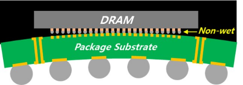
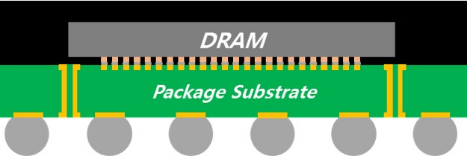
Flip chip board on chip (FCBOC) generally refers to a memory product where the distance between the chip and substrate is shortened by using bumps in order to minimize signal loss and increase transmission speed.
It is mainly used in DRAM chips that require mass production and high speed.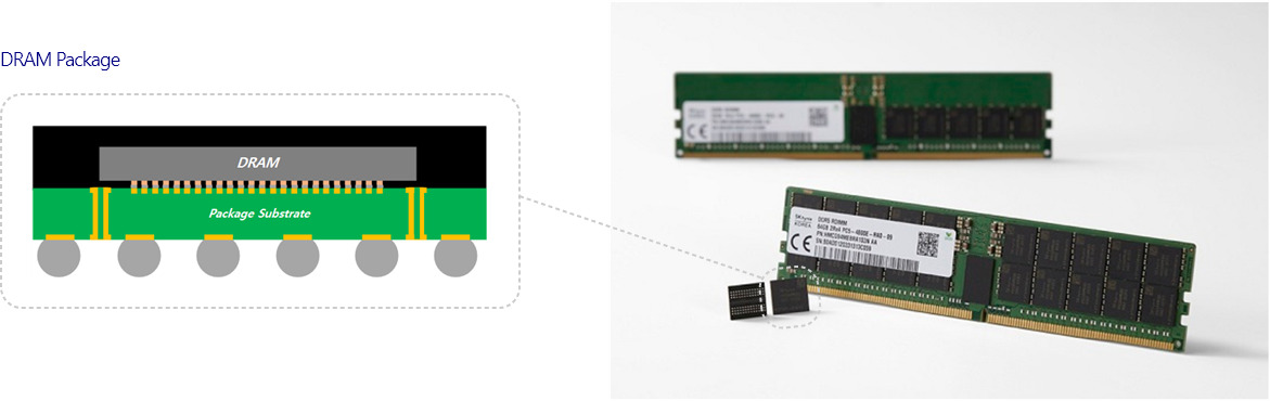
Key features
Low Dk Material
DRAM package with minimal signal loss can be made by using materials that have a low dielectric constant, and optimizing the processing method for the materials.Warpage Control
When warpage occurs in a board, a non-wetting defect occurs as the bump between the chip and board fails to bond. This can be prevented by preventing warpage through the manufacturing process and design.